Analog electronics
| Site: | central technical insititute.gnomio.com |
| Course: | central technical insititute.gnomio.com |
| Book: | Analog electronics |
| Printed by: | |
| Date: | Monday, 13 July 2026, 2:29 AM |
1. Network Analysis with d.c. Source
The components used in electronic circuits may be classified into two categories namely active and passive compo+nents. Active components are those which can perform signal processing functions such as signal generation, rectification and amplification. These components basically are semiconductor diodes, transistors and SCR’s etc. Batteries and generators which supply energy, also fall in the category of active components. The passive components are those which can not by themselves perform the above mentioned functions. The basic passive components are resistors, inductors and capacitors. In this chapter the analysis of electric circuits or networks, consisting of d.c. sources as the source of energy and other elements like resistors will be discussed using different methods. In addition different theorems will also be discussed to analyze complicated networks.
Before discussing the methods of analysis of network, it is necessary to give the model of the battery or the generator which supply energy to the network.
1.1. Model for a Battery:
: To discuss the model for the battery, consider a
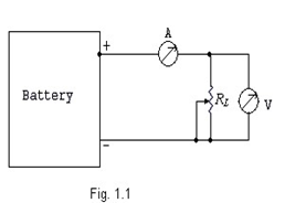
variable load resistance RL connected to the output terminals of the battery as shown in figure 1.1. Voltage across the load resistance is measured with the help of a voltmeter V. The current flowing through the load resistance RL is measured with the help of an ammeter connected in series with it. By varying the load resistance, the current I flowing through and the voltage across the load resistance RL is measured. A graph is plotted between the current I and voltage V as shown in figure (1.2). This is a straight line which cuts at V0 to the Y-axis and at I0 to the X-axis.
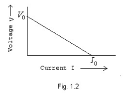
The equation for the straight line is of the form y=mx+C ,
V0
where m =− , is the slope of the curve
I 0
and C =V0 , is the intersect to the Y-axis.
V 0 V0
Thus V = −  I + V 0 ;
  has the dimension of resistance represented by R0.
I 0 I 0
This equation will be V = V 0 − R 0 I ------ (1.1)
The equivalent circuit of the equation (1.1) is given in figure (1.3).
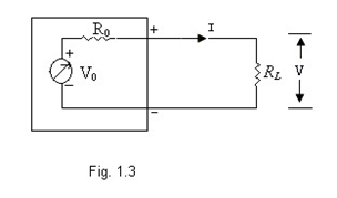
From this circuit, it is clear that the practical battery may be represented by a voltage source V0 and a resistance R0 in series with it. The resistance R0 is known as internal resistance, output resistance or source resistance of the battery.
Now put I = 0, i.e., the load resistance is removed from the circuit, then V = V0 and V0 is called as the open circuit voltage of the source. It is in fact the terminal voltage when no current is drawn from the source. The open circuit voltage when measured with a voltmeter will draw certain amount of current from the source. Thus open circuit voltage should be measured with an ideal voltmeter. Similarly, one more conceptual quantity called the short circuit current may be defined as the current flowing from the battery, when the external terminals of the battery are short circuited. The short circuit V0 current I0 will be equal to , since V = 0. This current can only be measured with an
I 0
ideal current meter. The ratio of open circuit voltage V0 to the short circuit current I0 is known as internal resistance of the battery.
From the model of the battery the following inferences can be drawn:
(i) If a load resistance RL is connected to a battery (fig. 1.4), then
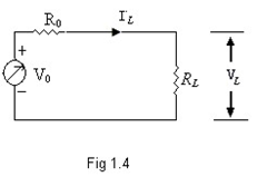
the load current IL is given by:
V 0
I L =  ------ (1.2)
(R 0 + RL )
The output voltage VL is given by:
 V0RL = V0 ------ (1.3) VL = I L RL = (R0 + RL ) (1 + R0 )
RL
 R 0 → 0 or R0 << RL , then VL = V0 ; the
From this equation it clear that if
R L
source will behave like an ideal voltage source. That is the source will said to be a good source if the internal resistance of the source is small enough than the load resistance. The ideal voltage source may be defined as follows:
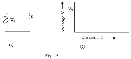
Ideal voltage source: An ideal voltage source is that source which provides a constant potential difference between its terminals, irrespective of the current drawn from it. An ideal voltage source is represented in figure 1.5(a) and it’s V – I relationship in figure 1.5(b).
(ii) Rewriting the equation (1.2), we get:
I L = ------ (1.4)
 R
R
(1 + ) (1 + )
0 R 0
It can be understood from this equation that the load current IL will be equal to the short
 RL → 0 or RL << R 0 ; the source will behave like an ideal circuit current, if the
R0
current source. That is the voltage source will act as a good current source if the source resistance is large enough than the load resistance. The current source is represented as short circuit current I0 and a source resistance R0 in parallel with it (fig.1.6). The ideal current source may be defined as follows:
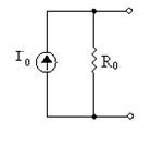 Fig. 1.6
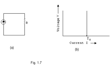
Ideal Current Source: An ideal current source is one which delivers a constant current in the circuit irrespective of the load connected to it. The V-I relationship of the ideal current source and its symbolic representation are shown in figure 1.7.
 |
(iii) Sometimes it becomes useful to transform or convert a voltage source into its equivalent current source or vice-versa. We equate the current flowing through the load resistance connected to both the circuits shown in fig. 1.8.
|
 From Current equivalent circuit I L = 0 0 L
(R 0 + R L )
V
 Equating these equations we have V0 = R0 I 0 or I 0 = 0
R 0
It is, therefore, concluded that the voltage source V0 with a series resistance R0 may be transformed to its equivalent current source I0 and the resistance R0 in parallel
 V 0 with it. The value of current source I0 is given by I 0 = . Similarly, a current source R 0
I0 with a resistance in parallel with it may be transformed to voltage source V0 and a resistance R0 in series with it. The value of voltage source is given by V0 = R0 I 0 .
Example 1.1 A variable load resistance is connected to the terminals of a battery. When the current flowing in the load is 2A, the voltage across the load resistance is 5.8 volts; also when the load current is 5A, the voltage across the load resistance is 5.5volts. All the measurements are made using ideal meters.
Find: (a) Open circuit voltage and source resistance of the battery.
(b) Equivalent current source model of the battery.
Solution: (a) Let V0 and R0 are the open circuit voltage and source resistance of the battery respectively. As per statement of the problem:
(i) 
 In the first case 5.8 volts = 2A RL or RL = 2.9 Ω; V0 RL = 5.8 or V0 .(2.9) = 5.8 or V0 = 2R0 + 5.8
and
(R0 + RL ) (R0 + 2.9)
In the second case 5.5volts = 5A.RL' or RL' = 1.1 Ω;
 and V0 RL' ' = 5.5 or V0 .(1.1) = 5.5 or V0
(R0 + RL ) (R0 +1.1)
From these two cases: V0 = 6 volts & R0 = 0.1 Ω.
= 5R0 + 5.5
(ii) The current source equivalent of the values calculated above is given in figure
(1.9). The value of current source I0 = 6 x .1 = 60 mA
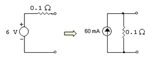
Fig. 1.9
1.2. Network analysis
The analysis of the electric circuits or networks which are formed by interconnecting the sources of electrical energy with other elements like resistances will now be discussed. Here consider the source of electrical energy as d.c. source which does not change with time. Simple circuits may be analyzed using well known Ohm’s law. Kirchoff’s laws may, however, be used to analyze more complicated circuits. Kirchoff presented two laws namely (i) Kirchoff’s Current law (KCL) & (ii) Kirchoff’s voltage law (KVL). These laws are the generalization of Ohm’s law.
1.2.1 Kirchoff’s Current Law (KCL): This law is applicable to any node or junction of electric circuit. The node or junction in an electric circuit is defined as the point where more than two elements meet. This law states that the algebraic sum of currents entering to any node of an electric circuit is zero. The total current entering to a node must be equal to that leaving it. The sign convention for this law is generally assumed that the current entering the node is positive while the current leaving the junction is negative. Mathematically, the law is ∑I = 0 .
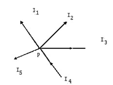
Fig. 1.10
This law may further be illustrated by considering the junction P shown in figure 1.10. I1, I2 & I5 are the currents entering the junction which are assumed to be positive while I3, & I4 are negative, as these are leaving the junction.
So I1 + I 2 − I 3 − I 4 + I 5 = 0
or I 1 + I 2 + I 5 = I 3 + I 4
Current leaving = Current entering
1.2.2 Kirchoff’s Voltage Law (KVL): This law is applicable to a mesh or loop of an electric circuit. A mesh or loop is defined as a closed circuit. The Kirchoff’s Voltage law states that the algebraic sum of all the voltage drops in any loop is zero.
The sign convention for applying the KVL to the closed loop is that an arbitrary reference direction of current in the clock wise direction is assumed. The associated reference direction across the resistances is marked positive at the tail of the arrow and negative to head of the arrow. If there is a voltage drop in the circuit, it is assumed to be positive while it is assumed to be negative for the voltage rise in the circuit.
For applying the KVL, we consider a closed circuit given the figure 1.11
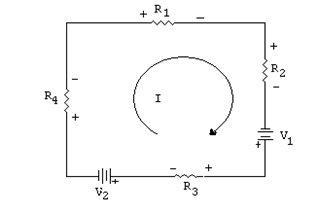
Fig 1.11
From this figure: R I1 + R2 I −V1 + R I3 +V2 + R I4 = 0 or (R1 + R2 + R3 + R4 )I =V1 −V2
From this equation it is clear that any unknown quantity may be calculated if rest of the quantities is known.
Example 1.2 A voltmeter having the sensitivity of 20KΩ/V is used to measure the voltage across 50KΩ resistance in the circuit shown in the figure (1.12). The voltmeter is used in 50volts range.
Calculate (a) the reading of the voltmeter,
(b) percentage error in the reading with respect to true value.
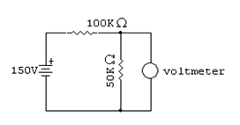
Fig. 1.12
150x50K
Solution: The true voltage =  = 50 volts (100 + 50)K
Resistance of the voltmeter in 50volt scale is
Rg =50x20K = 1MΩ
When the voltage across 50KΩ resistance is measured, the voltmeter resistance Rg will also come in parallel with 50KΩ resistance. So the voltage will be measured across the parallel combination and not across 50 KΩ resistance. Due to which there will be an error.
Reading of the voltmeter Vm will be equal to the voltage across the parallel combination. Resistance of the parallel combination is given by:
50Kx1M
Req = = 47.6KΩ
(1M + 50K)
Voltmeter reading Vm = = 48.36volts
% error in the reading = = 3.28%
1.3. Mesh and Node Method
2. Two – Port Network
A network contains active and passive elements connected in the form of a circuit.
Usually, a network has one pair of terminals for Input and other pair for the output. A pair of Input terminals of the network is called as Input port and the pair of the output terminals is called as the output port. Such a network is called as two port network. If the elements in the network are linear, the network is known as linear two port network. To understand the characteristics or to analyse a linear two port network, consider a black box as shown in figure 2.1. The 1, 1 terminals of the black box is known as input port and 2, 2 terminals is known as output port.
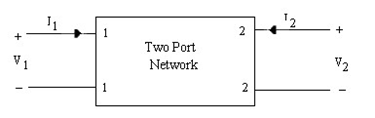
Fig. 2.1
In this network V1, I1 are the Input voltage and current; and V2, I2 are the output voltage and current. Any pair of variables may be arbitrarily chosen as independent variables, and other variables (dependent variables) may be obtained as a function of independent variables that is dependents variables may assumed to be the functions of independent variables.
2.1. Impedance parameters
A linear two port network represented by black box is considered, having I1 and I2 as independent variables and V1 and V2 as dependent variables.
V1 = f1 ( I1, I2 )
V2 = f2 ( I1, I2 ) ------ (2.1)
The changes in the dependent variables may be given by:
∂V ∂V
 dV 1dI 1dI 2 ∂I ∂I
|
dV 2 |
= |
|
dI 1 + |
|
dI 2 ------ (2.2) |
The partial derivatives in these equations become constant with operation over linear region of the device curve with constant slope.
The equations may, therefore, be written as:
V 1 = Z 11 I 1 + Z 12 I 2
V 2 = Z 21 I 1 + Z 22 I 2 ------ (2.3)
In the matrix form it is given by:
V1 Z 11 Z 12 I 1
=
------ (2.4)
V 2 Z 21 Z 22 I 2
Where Z’s are the impedance (resistance for d. c.) parameters, which may be defined as:
Z 11 =, is the input impedance when output is open
I 2 = 0
circuited or open- circuit input impedance.
Z 12 = , is the reverse transfer impedance when
I 1 = 0
input is open circuited or open circuit reverse transfer impedance.
Z 21 =, is the forward transfer impedance when
I 2 = 0
output is open circuited or open circuit forward transfer impedance. and Z 22 =, is the output impedance when input is open
I 1 = 0
circuited or open circuit output impedance.
These Z parameters also known as open circuit parameters, since in these parameters either input or output is open circuited. The equivalent circuit of the network using Z- parameters may be drawn as given below:
2.2. Admittance Parameters
: The admittance parameters of a linear two port network may also be defined in the similar fashion as the impedance parameters discussed above. In the admittance parameters, variables V1 & V2 are assumed independent variables and I1 & I2 as the dependent variables. The dependent variables I1 & I2 may be defined as a linear function of Independent variables V1 & V2 as
I1 = f1 ( V1, V2 )
I2 = f2 ( V1, V2 ) ------- (2.5)
and I1 =Y11V1 +Y12V2
I2 =Y21V1 +Y22V2 ------- (2.6)
In the matrix form it is given by :
I1 Y11 Y12 V1
= ------ (2.7)
I 2 Y21 Y22 V2
Where Y’s are the admittance (conductance for d. c.) parameters, which may be defined as :
Y 11 =, is the input admittance when output is short
V 2 = 0
 circuited or short- circuit input admittance.
Y 12 = , is the reverse transfer admittance when input is
V 1 = 0
short circuited or short circuit reverse transfer admittance.
Y 21 =, is the forward transfer admittance when output is
V 2 = 0
short circuited or short circuit forward transfer admittance.
and Y 22 = , is the output admittance when input is short
V 1 = 0
circuited or short circuit output admittance.
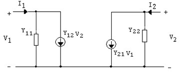
These Y – parameters are also called as short circuit parameters as given in the network either input or output is shorted. The equivalent circuit of the network using Y- parameters is given in figure2.3.
2.3. Hybrid parameters
3. Networks with Time Varying Sources
So far the analysis of networks containing only batteries and resistances has been discussed. In this chapter the network with time varying sources, resistances and other elements like inductances capacitances and transformers, etc. will also be discussed. The time varying sources are generally of three types, viz., periodic, aperiodic and random. Sine, Square and Triangular waves are periodic, since it repeats after a fixed interval of time. Periodic waves are generally used in the electronic circuits and are of our great interest. A pulse is aperiodic and noise is of random nature
3.1. Fourier series
:
: Any function f(t) can be expanded using Fourier series, which is expressed as the summation of sinusoidal (sine, cosine or both) terms as given by:
∞ ∞
|
f |
A0 + ∑ A n Sin (nωt ) + ∑ B n cos( n=1 n=1 |
nωt ) |
------- (3.1) |
|
where |
1 T A0 = T 0 T |
|
------ (3.2) |
2
An dt ------ (3.3)
2 T
Bn dt ------ (3.4)
Example 3.1 Find the first four coefficients of the half wave rectified output, using Fourier series expansion. Characteristics of the wave are:
f t = EmSinωt when 0 ≤ t ≤ T / 2 f t
= 0 T / 2 ≤ t ≤ T
Solution: The coefficients of Fourier series of the half wave rectified output wave are given as:
1 T 1 T / 2 T
A0 = ∫EmSin(ωt).dt = ∫EmSin(ωt dt) + ∫(0).dt
T 0 T 0 T / 2
E
|
= |
|
------ (3.5) |
|
2 T / 2 An = |
|
------ (3.6) |
T 0
2Em T / 2
= ∫[Cos(n −1)ωt −Cos(n +1)ωt dt]
T 0
 = 2E2πmωSinn(n−−1)1)ωωt − Sin(n(n++1)1)ωωt T0 / 2
(
E Sin (n −1)π Sin (n + 1)π

 (n −1) − (n + 1)
= 0 (for all values of n, except for n = 1)
For n = 1 denominator of the above equation will be inderminent. So we calculate A1 by putting n = 1 directly in equation (3.6) as:
2 T / 2
A1 =  ∫ Em Sinωt.Sinωt dt. T 0
2Em T / 2 2 2Em T /2
= ∫Sin ωt dt. = ∫[1−Cos2ωt dt]
T 0 2T 0
Em T Sin2ωtT / 2 Em T
= T 2 − 2ω 0 = T 2 − 0
Em
= ------ (3.7)
2
Bn may be calculated as:
2 T / 2
Bn = ∫EmSin( . ).ωt Cos(nω. ).t dt T 0
2Em T / 2 −Sin(n−1) .ωt+Sin(n+1) .ωt
= ∫0 2 dt
T
EmωCos(n−1)ωt Cos(n +1)ωtT / 2
= 2 −1)ω − (n +1)ω 0
π (n
Em Cos(n −1)π Cos(n +1)π 1 1
 = −1) − (n +1) − (n −1) + (n +1)
2π (n
Em 1 1 1 1
 If n is odd, then Bn = π −1) − (n +1) − (n −1) + (n +1) = 0 ------ (3.8)
2 (n
Em 1 1 1 1
 If n is even, then Bn = 2 − −1) + (n +1) − (n −1) + (n +1) π (n
2Em 1 1
 = 2π − (n −1) + (n +1)
Em − n −1+ n −1 2Em
 = 2 =− 2 ------- (3.9)
π (n −1) (n −1)π
(where n is even i.e. n = 2,4,6,8…..)
So by putting the values of A’s and B’s in equation 3.1 we get the required function for half wave rectified output as:
Em Em 2Em 2Em 2Em
E = + Sinωt −  Cos2ωt −
  Cos4ωt − Cos6ωt........ ------- (3.10) π 2 3π 15π 35π
Example 3.2 Consider a full wave rectified signal of peak value Em and period T. Find its coefficients in the Fourier series expansion.
Solution: The coefficients of Fourier series of the full wave rectified output wave are given as:
1 T 1 T / 2 T
A0 = ∫EmSin(nωt).dt =  ∫EmSin(ωt dt) + ∫
 − EmSin( . )ωt dt T 0 T 0 T / 2

 m ------ (3.11)
2 T / 2 T
An =  ∫EmSin(ωt).Sin(nωt).dt + ∫EmSin(ωt).Sin(nωt).dt
T 0 T / 2
4Em T / 2
=  ∫Sin(ωt).Sin(nωt).dt T 0
4Em T / 2
=  ∫[Cos(n −1)ωt −Cos(n +1)ωt dt]
2T 0
2EmωCos (n −1)ωt Cos (n + 1)ωt T / 2
 = 2π (n −1)ω − (n + 1)ω 0
Em Sin(n −1)π− Sin0 Sin(n +1)π+ Sin0
 = π (n −1) − (n +1)
Em Sin(n −1)π Sin(n +1)π
 = π −1) − (n +1) = 0 ------ (3.12) (n
2x2 T / 2
Bn =  ∫EmSin( . ).ωt Cos(nω. ).t dt
T 0
4Em T / 2 − Sin(n−1) .ωt + Sin(n+1) .ωt
 = ∫0 2 dt
T
2EmωCos(n −1)ωt Cos(n +1)ωtT / 2
 = 2π (n −1)ω − (n +1)ω 0
Em Cos(n −1)π Cos(n +1)π 1 1
 = −1) − (n +1) − (n −1) + (n +1) π (n
Em 1 1 1 1
 If n is odd, then Bn = π (n −1) − (n +1) − (n −1) + (n +1) = 0 ----- (3.13)
Em 1 1 1 1
 If n is even, then Bn = − −1) + (n +1) − (n −1) + (n +1) π (n
2Em 1 1
 = 2 − −1) + (n +1) π (n
2Em − n −1+ n −1 4Em
 = 2 =− 2 ------- (3.14) π (n −1) (n −1)π
(where n is even i.e. n = 2, 4, 6, 8…..)
So by putting the values of A’s and B’s in equation 3.1, the required function for full wave rectified output is obtained as:
2Em 4Em 4Em 4Em
 E = − Cos2ωt − Cos4ωt − Cos6ωt........ ------- (3.15) π 3π 15π 35π
Example 3.3 Consider a symmetrical triangular wave of peak value Em and period T as shown in figure (3.1). Find its coefficients in the Fourier series.
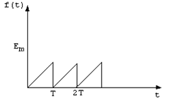
Fig. 3.1
Solution: let f(t) = X + Y.t at t = 0 f(t) = 0 So X = 0 at t = T f(t) = Em
Em = Y T or Y = (Em)/T
Em f t = ( ).t is the equation of the triangular wave. So the coefficients of
T
Fourier series of this wave are given as:
1 T Em Em T 2 Em

 A0 = ∫ . .t dt = 2 = ------ (3.16)
T 0 T T 2 2
An = 2 T∫ Em . .t Sin(nωt).dt
T 0 T
2E T
 =
=  t dt
t dt
T 0
2Em −tCos(nωt) T 1.Cos(nωt)
 = 2 +∫ .dt T nω 0 nω
2Em −tCos(nωt) Sin(nωt)T
 = 2 nω + n 2ω2 0
T
2Em −TCos(2nπ) Sin(2nπ)
 = T 2 nω + n 2ω2
2Em TCos(2nπ) 2Em
 =− T 2 nω =− nω Cos2nπ
Em
=− (since Cos 2nπ=1 for all values of n) nπ
Bn = 2 T∫ Em . .t Cos(nωt).dt
T 0 T
2Em tSin(nωt) T 1.Sin(nωt)
 = 2 −∫ .dt
T nω 0 nω
2Em tSin(nωt) Cos(nωt)T
 = 2 nω + n 2ω2 0
T
2Em TSin(2nπ) Cos(2nπ) 1
 = 2 nω + n 2ω2 − n 2ω2
T
=  22E2m 2 [Cos(2nπ) −1]=
  2E2 m 2 [1−1]= 0 ------ (3.17) n ω T 2n π
So by putting the values of A’s and B’s in equation 3.1, the required Fourier series of the
Em Em Em Em triangular wave is as: E = − Sinωt − Sin2ωt − Sin3ωt........
2 π 2π 3π
Example 3.4 Find the Fourier series expansion of the square wave shown in figure (3.2).
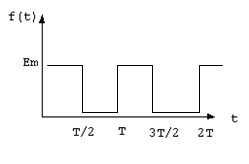
Fig. 3.2
Solution: The coefficients of Fourier series of the square wave are defined as:
1 T 1 T / 2 T
A0 = ∫ f t.dt =
∫Emdt + ∫(0)dt
T 0 T 0 T / 2
E m T E m
 = 2 = 2
T

 2 T∫/ 2 T∫ 2Em [−Cos(nωt)]T0 / 2
An = Em.Sin(nωt).dt + (0).Sin(nωt).dt=
T 0 T / 2 nωT
2Em
= (  )1[ −Cos(nωT / 2)] nωT
2Em
= ( )[1−Cos(nπ)] = 0 for even values of n nπ
2Em
= (  ) for odd values of n nπ
2 T / 2 T
Bn = ∫Em.Cos(nω. ).t dt + ∫(0)Cos(nωt).dt T 0 T / 2
2Em T / 2 2Em nωT Em
 = (
= (  )[Sin(nωt)]o = ( )Sin( ) = Sin(nπ) = 0 for all values of n. nωT nωT 2 nπ
So by putting the values of A’s and B’s in this equation, the required Fourier series of the Square wave is given as:
Em 2Em 2Em 2Em 2Em f t = +
Sin(ωt) + Sin(3ωt) + Sin(5ωt) + Sin(7ωt) +....
2 π 3π 5π 7π
3.2. Sinusoidal Signal applied to different elements
When an A.C. signal E t = EmSinωt is applied to a simple resistance, according to Ohm’s Law one may obtain the instantaneous value of the current flowing through the circuit as:
E t E m
I t = = Sin ωt
R R
= I m Sin ωt (Im is the peak value of current)
Thus the current wave form is the exact replica of the voltage, i.e., both are in the same phase. But when an A.C. source is applied to any combination of resistance, inductance and capacitance, we get the current and voltage are having certain phase difference. Phase relation between the current flowing through and voltage applied across the circuit may best be understood if the Impedances and reactances are represented on the complex plain.
When an A.C. signal E t = E m Sin ωt is applied across an inductance L, the instantaneous value of the current flowing through the circuit is given by:
1 1
I t =
∫ E .t dt =
∫ (E m sin ωt).dt
L L
= E m . − cos ωt = E m sin ωt − π ------ (3.18)
L ω ωL 2
It is clear from this equation that the current is lagging by an angle of 90 o with the voltage. The quantity Em is known as the peak value of the current. It is
ωL
customary to represent the magnitude as well as the phase relation between the voltage and the current in a graphical form. Such a graphical form is known as phasor diagram.
The phasor diagram is generally represented on the complex plain, as shown in figure (3.3). When a quantity coincides with the X-axis (real axis), it is known as real quantity. The quantity on X-axis when multiplied by j (( j = −1) , makes it purely imaginary quantity. It rotates by an angle of 90o in the anti-clock wise direction. However, when the real quantity is divided by j or multiplied by (– j) it rotates in the clock wise direction by 90o.
Fig. 3.3
From the equation (3.18), it is clear that the voltage E, when divided by ωL , the correct magnitude of the current is obtained. In order to rotate the phase by – 90 o the magnitude of current is further divided by j as:
E π
I = and ∠I =∠E − jωL 2
The imaginary quantity ( jωL) is called the inductive reactance of the inductance L.
The current is lagging behind the voltage by an angle of 90o as shown in figure (3.4). This is the phase relation between the current and voltage.

I
Fig. 3.4
1 − j
Similarly the reactance of a capacitance is or , which is also an jωC ωC
imaginary quantity represented on the imaginary axis. The current flowing through the capacitance C when an A.C. signal of voltage E is applied across the capacitance is given
E
by: I == jωCE
(1 jωC)
or 
The current is 90o ahead by the voltage as is shown in figure (3.5).
I
E
Fig. 3.5
The impedance of a series combination of a resistance R and an inductance L is given by Z = R + jωL or Z = R 2 + (ωL) 2
The phase angle θ the impedance makes with the resistive component R is given by: θ= tan−1 (ωL) R
The impedance Z is written as: Z = Z .∠tan−1 (ωL)
R
The current flowing through this combination is given by:
I = E = E or ∠I =∠E − tan−1 (ωL)
Z R + jωL R
The current is lagging behind with the voltage by an angle tan−1 (ωL).
R
The impedance of a series combination of a resistance R and an capacitance C is
1 2 2 given by Z = R + or Z = R + (1 ωC) jωC
The phase angle θ the impedance makes with the resistive component R is given
by: θ= tan−1 ( 1 )
ωCR
The impedance Z is written as: Z = Z .∠tan−1 ( 1 ) ωCR
The current flowing through this combination is given by:
E E E.( jωC) π −1
I = = = or ∠I =∠E + − tan (ωCR)
Z R + (1/ jωC) 1+ jωCR 2
The phase difference between current and voltage is − tan−1 (ωCR) .
Example 3.5 An A.C. signal of 20 volts and frequency 200Hz as applied to a circuit consisting of 10 mH inductance and 10 Ω resistance in series with it. Find the magnitude and phase of the current.
Solution: The impedance Z of series combination is given by:
Z = R + j2.πf L. = 10 + jx2x3.14 x200 x10 x10 −3 = 10 + jx12.56
Z = (10) 2 + (12.56) 2 =16Ω and θ= tan−1 () = 51.47 0
Current =1.25amp
Fig. 3.6
And phase difference ϕ=∠I −∠V =−51.47 0
Example 3.6 Consider a series R – C circuit having R = 1.5KΩ and C = 0.2µF is excited by a sinusoidal signal of 20 volts and frequency 2 KHz. Find the magnitude and phase of the current.
Solution: The impedance of the R – C circuit is given by: j j
Z = R −ωC =1500 − 2x3.14x2000x0.2x10−6
j104
=1500 − =1500 − j398.1
25.12
Z = (1500) 2 + (398.1) 2 =1552Ω
So Z =1552Ω∠−14.860
Fig. 3.7
The phasor diagram is given in figure 3.7.
Example 3.7 Consider a sinusoidal signal of peak value of 20 volts with frequency of 2000 radians/sec is applied to a circuit shown in figure (3.8). L=20 mH, C1=C2=0.2 µF, R=100 Ω . Calculate the total current I and the currents I1 & I2 in the two branches.
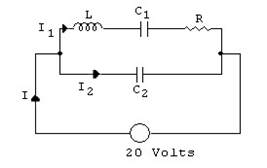
Fig. 3.8
Solution: Impedance Z1 of the series branch is given by:
Z
Current I1 in this series branch is given by:
20 20 0
I1 = = 0 = 8.13mA∠87.67 Z1 2.46KΩ∠−87.67
− j − j − j104
Impedance of the capacitor branch Z 2 =ωC2 = 2000x0.2x10−6 = 4
|
|
=−2500 j = 2.5KΩ∠−π/ 2 |
|
Current I2 in this branch is given by: |
|
I / 2
/ 2
Admittance of Z1 & Z2 impedances is given by:
1 1 1 1 1
Y = = + = 0 +
Z Z1 Z 2 2.46KΩ∠−87.67 2.5KΩ∠−π/2
= 0.00041∠87.67 0 + 0.0004∠π/2
= [0.000017 + j0.00081]+[ 0.j 0004] = 0.000017 + j0.00081
= 0.00081∠88.80
Total impedance Z 
Total current I